As its name implies, non-linearity is the difference between the graph of the input measurement versus actual voltage and the straight line of an “ideal” measurement. The non-linearity error is composed of two components, integral non-linearity (INL) and differential non linearity (DNL). Of the two, integral non-linearity is typically the specification of importance in most data acquisition (DAQ) systems.
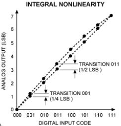
INL is the maximum deviation between the ideal output of a DAC and the actual output level (after offset and gain errors have been removed).
INL: The specification is commonly provided in “bits” and describes the maximum error contribution due to the deviation of the voltage versus reading curve from a straight line. Though a somewhat difficult concept to describe textually, INL is easily described graphically and is depicted in Figure 4. Depending on the type of A/D converter used, the INL specification can range from less than 1 LSB to many, or even tens, of LSBs.
DNL: Differential non-linearity describes the “jitter” between the input voltage differential required for the A/D converter to increase (or decrease) by one bit. The output of an ideal A/D converter will increment (or decrement) one LSB each time the input voltage increases (or decreases) by an amount exactly equal to the system resolution.
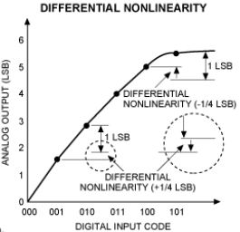
DNL is the deviation between two analog values corresponding to adjacent input digital values.
For example, in a 24-bit system with a 10-volt input range, the resolution per bit is 0.596 microvolt. Real A/D converters, however, are not ideal and the voltage change required to increase or decrease the digital output varies. DNL is typically ±1 LSB or less. A DNL specification greater than ±1 LSB indicates it is possible for there to be “missing” codes. Though not as problematic as a non-monotonic D/A converter, A/D missing codes do compromise measurement accuracy.
Check out UEI’s Master Class Videos on Youtube.


